 |
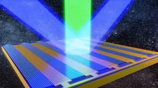
| In this rendering of a new optical metasurface, a laser beam (green) hits the surface, which creates steerable beams of light at different frequencies (blue) Image credit: Caltech |
A New Era of Light Manipulation: The Power of Metasurfaces
A groundbreaking tunable smart surface has been developed that can transform a single pulse of light into multiple beams, each directed in different directions. This proof-of-concept innovation is set to revolutionize fields such as communication, imaging, sensing, and medicine.
How the Metasurface Works: Nanostructures and Light Control
The innovation stems from the Caltech lab of Professor Harry Atwater, who specializes in applied physics and materials science. The key to this development is a type of nano-engineered material known as a metasurface. According to Prachi Thureja, a graduate student in Atwater’s group, “These are artificially designed surfaces consisting of nanostructured patterns. Each nanostructure allows us to locally control the properties of light.”
What sets this surface apart is its ability to be reconfigured up to millions of times per second, enabling rapid manipulation and redirection of light. This capability opens up applications in optical data transmission, including optical space communications and Li-Fi, as well as in lidar technology.
Beyond Lenses and Mirrors: Electrically Reprogrammable Light Control
Traditional methods of manipulating light rely on conventional lenses and mirrors that utilize Snell’s Law to direct light based on the optical properties of materials. However, this new metasurface eliminates the need for these bulky components. Instead, it uses a semiconducting material combined with nano-scale mirror elements to achieve similar effects, all within a flat, microscopic device.
By applying different voltages across the device, the metasurface can change the profile of light without any physical movement. Jared Sisler, a co-author of the study and another graduate student in Atwater’s group, explains, “We can steer the light like it’s an electrically reprogrammable mirror.”
The Metasurface Device: Design and Functionality
The device itself is a chip measuring 120 micrometers on each side, equipped with an embedded surface of tiny gold antennas within a semiconductor layer of indium tin oxide. By adjusting the voltages across the semiconductor, the device can alter its index of refraction, thus bending light in new ways. The combination of the reflective gold mirror elements and the tunable refractive capacity of the semiconductor allows for highly adaptable light manipulation.
Unlocking New Possibilities with Metasurfaces
The potential of this technology extends far beyond its initial demonstration. As Alex M.H. Wong, an associate professor of electrical engineering at the City University of Hong Kong, notes, "The metasurface can be flat, ultrathin, and lightweight while achieving functions typically requiring a series of carefully curved lenses." Wong also emphasizes that scientists are just beginning to unlock the vast possibilities metasurfaces offer, with applications across communication, imaging, sensing, and medicine.
With advancements in nanofabrication, metasurfaces are becoming increasingly viable for real-world use. Industry players are already making significant investments in pushing this technology toward commercialization, signaling a future where metasurfaces could become a cornerstone in various technological fields.


0 Comments